製品紹介
TANOSYSTEM CO.,LTD
TANOSYSTEM CO.,LTD
Polished Wafer is a thin disc-shaped single crystal silicon substrate manufactured from high-purity poly-crystalline silicon by series of melting, crystal growth, cutting, polishing and washing processes. It is the most common wafer used to manufacture semiconductor chips.
| Specification | 100 mm | 125 mm | 150 mm | |
|---|---|---|---|---|
| Type [Dopant] | P | Boron | ||
| N | Phosphorus [P], Red-Phosphorus, Antimony [Sb], Arsenic [As] | |||
| Resistivity (Ω · cm) | P | 0.001 ~ 100 | ||
| N | 0.001 ~ 100 | |||
| Thickness (μm) | 525±25 | 525±25 | 625±25 | |
| 675±25 | ||||
| Warp (μm) | Max 30 | |||
| TTV (μm) | Max 30 | |||
- Available in customized specs for specific needs. ex) 150mm, N[As], Thickness-375±10μm
| Specification | 200 mm | 300 mm | |
|---|---|---|---|
| Type [Dopant] | P | Boron | |
| N | Phosphorus [P], Antimony [Sb], Arsenic [As] | ||
| Resistivity (Ω · cm) | P | 0.001~100 | |
| N | |||
| Warp (μm) | 725±25 | 725±25 | |
| Thickness (μm) | Max 50 | Max 30 | |
| TTV (μm) | Max 30 | Max 5 | |
- Additional product line-ups are ready upon customer’s request. ex) Particle, Resistivity, Flat or Notch etc.
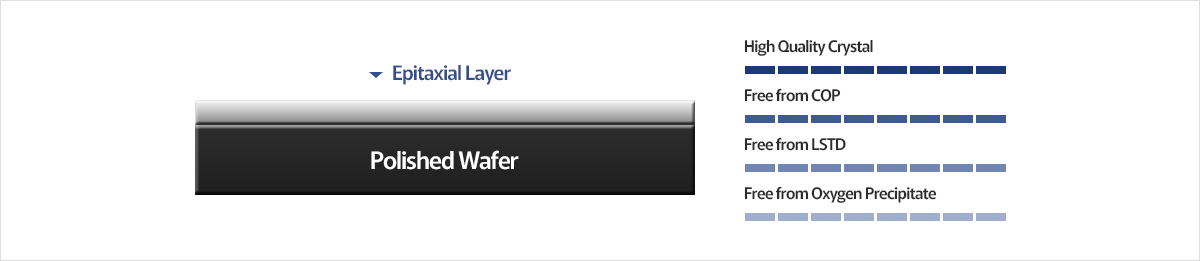
Epitaxial Wafer has a single crystal silicon layer on top of single crystal silicon substrate (Polished Wafer). They both have the same crystal structure, but Epitaxial layer differs in physical properties such as dropping, band gap and permittivity properties, yielding less defect density than the substrate. Therefore, it has superior structural and electrical properties to the original Polished Wafer, making it possible to improve performance on manufacturing extensive semiconductor devices.
| Specification | 200 mm | 300 mm | |
|---|---|---|---|
| Type [Dopant] | P | Boron | |
| N | Phosphorus [P], Antimony [Sb] | ||
| Resistivity (Ω · cm) | Sub | 0.001~100 | |
| EPI | 0.1~50 | ||
| EPI Thickness (μm) | 1~100 | ||
| Warp (μm) | Max 10 | ||
| TTV (μm) | Max 10 | ||
- Additional product line-ups are ready upon customer’s request. ex) Particle, Resistivity, Flat or Notch etc.
Float Zone (FZ) crystal growing method is one of the first attempted approaches on Ingot growing, initially developed in the early 1960s. FZ method is characterized by high resistivity value and low oxygen concentration, which are mandatory for high purified single crystal manufacturing.
| Specification | 100 mm | 125 mm | 150 mm | 200 mm | |
|---|---|---|---|---|---|
| Type [Dopant] | P | Boron | |||
| N | Phosphorus [P] | ||||
| Resistivity (Ω · cm) | P | 1,000 ~ 15,000 | |||
| N | |||||
| Thickness (μm) | 525±25 | 525±25 | 625±25 | 725±25 | |
| 625±25 | |||||
| TTV (μm) | Max 10 | ||||
- Additional product line-ups are ready upon customer’s request
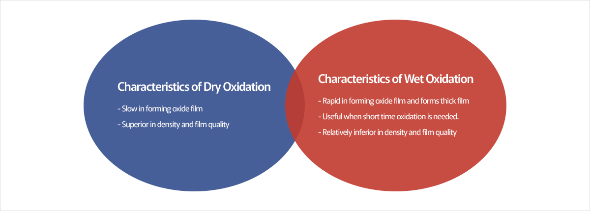
Oxidation Wafer Oxidation Wafer is an electrical insulator wafer, processed at a high temperature, which allows Polished Wafer to have oxide film on its surface. It is used as a field oxide for electrical insulating gate of MOS transistors and other various structures inside chips. Oxidation is done in either Dry or Wet methods. The characteristics of each type are on the following diagram.
Metal Deposition Wafer Metal Deposition Wafer is coated with variety of metal films for semiconductor manufacturing. According to a specific process, Copper (Cu), Nickel (Ni), Tungsten (W) and various metals are deposited on the Wafer.
Glass wafer is thin discs of precision glass, made of borosilicate, fused silica, glass, and quartz. It is essential for display engineering and display glass inspection systems. Also, glass wafer is used as a substrate carrier for bonding silicon or other substrates, for Micro Electro Mechanical Systems (MEMs).
Glass wafer is superior to the regular substrate in certain aspects. While being more cost-effective, it has better wrap management and less electrical loss. The glass wafer market is expected to grow further since its related industries like IoT are rapidly expanding.
| Unit | D 263® T eco | AF 32® eco | SCHOTT®AF 35 G | B 270® i | BOROFLOAT® 33 BOROFLOAT® 33 HT |
BOROFLOAT® 40 | |
|---|---|---|---|---|---|---|---|
| Optical Properties | |||||||
| Refractive index nD | as drawn | 1.5230 | 1.5099 | 1.5100 | 1.5229 | 1.4714 | 1.486 |
| Luminous Transmittance tvD65 | % (at thickness) | 91.7 (0.3 mm) | 92.1 (0.4 mm) | 92.1 (0.7 mm) | 91.7 (2 mm) | 92.7 (1.1 mm) | to be checked |
| Thermal Properties | |||||||
| CTEα | 10-6K-1 (20 °C, 300 °C) | 7.2 | 3.2 | 3.3 | 9.4 | 3.25 | 4.15 |
| Transformation temperature Tg | °C | 557 | 717 | 712 | 542 | 525 | 589 |
| Mechanical Properties | |||||||
| Densityρ | g/cm³ | 2.51 | 2.43 | 2.40 | 2.56 | 2.23 | 2.31 |
| Young´s modulus E | kN/mm² | 72.9 | 74.8 | 73.9 | 71.0 | 64.0 | 69.0 |
| Chemical Properties | |||||||
| Hydrolytic resistance | Class ISO 719 | HGB 1 | HGB 1 | HGB 1 | HGB 3 | HGB 1 | HGB 1 |
| Acid resistance | Class DIN 12116 | S 3 | S 4 | S 4 | S 2 | S 1 | S 1 |
| Alkali resistance | Class DIN ISO 695 | A 2 | A 3 | A 3 | A 1 | A 2 | A 2 |
| Electrical Properties | |||||||
| Dielectric constant εr (at 9 = 25 °C) | 1 GHz | 6.4 | 5.1 | 5.2 | 6.7 | 4.5 | to be checked |
| Young´s modulus E | 1 GHz | 74·10 -4 | 35·10 -4 | 38·10 -4 | 59·10 -4 | 51·10 -4 | to be checked |
〒475-0075 愛知県半田市苗代町2丁目36-3
TEL/FAX : 0569-47-7615
E-mail : info@tanosystem.com
Copyright ⓒ
2021 TANOSYSTEM CO.,LTD.
all rights reserved.
